End the "Grid Effect"! Unveiling SPECTRUM's LED Chip Relocation Visual Seamless Technology
[Introduction] In the actual application and deployment of kinetic screens, one of the most persistent headaches faced by engineers, exhibition contractors, and visual designers is: What should we do if the kinetic screen gaps are too large?
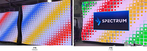
Because every module in a kinetic screen needs to perform independent, high-frequency physical extensions on the Z-axis, traditional structural designs must reserve substantial physical gaps (usually 3mm to 5mm or more) between modules to prevent them from rubbing or colliding at high speeds. This physical compromise directly results in a screen covered with harsh black grid lines when lit up. The imagery suffers from a severe "fragmented effect," completely destroying the immersive and premium feel of the digital art.
Facing this industry-wide pain point, SPECTRUM, a comprehensive service provider of dynamic display systems and spatial digital equipment, has delivered a hardcore engineering answer: our proprietary LED Chip Relocation Visual Seamless Technology.
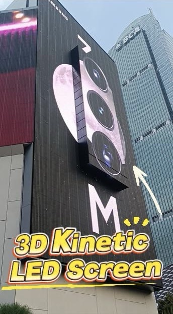
I. Principle Analysis: What is LED Chip Relocation?
Many clients wonder: since physical gaps cannot be eliminated for safety reasons, how does SPECTRUM make the "seams disappear"? The answer lies in the optical-level reconstruction of the PCB Surface-Mount Technology (SMT) process.
In traditional LED modules, all LED chips are arranged in an absolutely equidistant matrix on the PCB. The chips on the edge maintain a standard safety distance from the physical edge of the module.
SPECTRUM's pioneering LED Chip Relocation technology breaks this convention. When designing the module PCB, our hardware R&D team utilizes extreme-precision SMT processes to apply a micro-level "outward shift" to the outermost ring (or rings) of LED chips, pushing them directly toward the physical edge of the module.
II. Optical Ingenuity: Compressing the Seam to an Extreme 0.9mm
The brilliance of this technology lies in its ability to create the ultimate "optical illusion":
On the Physical Level: The die-cast aluminum bottom shell and the side anti-collision structures of the modules still maintain ample safety clearances. This ensures that even when the equipment moves at speeds up to 500mm/s, the modules do not interfere with each other and operate with silky smoothness.
On the Visual Level: When the matrix screen is on the same flat plane, or when adjacent modules form an undulation, the light-emitting points of adjacent modules are pulled extremely close together because the edge chips have been pushed outward.
Through this physical coverage at the light-emitting layer, the originally glaring black gaps are filled with light. SPECTRUM has successfully compressed the physical gap visually to under 0.9mm! On certain flagship models (like the indoor SPKI-128 and the outdoor SPKO-500), it even achieves a near 0mm visual seamless effect.
III. Experience Elevation: Reshaping the Premium Feel of 3D Kinetic Vision
A visual seamless kinetic screen brings more than just a spec upgrade; it delivers a "dimensional strike" across various application scenarios:
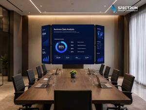
Flawless High-Density Information Display: In science museums or corporate showrooms, when a kinetic screen needs to display precise data charts, small text, or high-fidelity 3D product modeling, the 0.9mm visual micro-seam ensures line continuity. Text and data are no longer rigidly sliced by black lines.
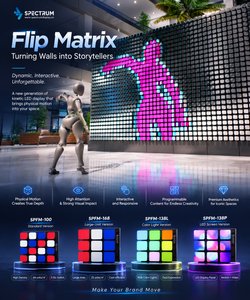
Ultra-Realistic Dynamic Naked-Eye 3D: When hundreds or thousands of modules form 3D shapes , the ultimate micro-seam technology makes the entire kinetic surface as smooth as fluid. It truly achieves top-tier visual art that "cuts space, but never cuts the picture."
💡**FAQ **
__
Q1: During project design, what should we do if the kinetic screen gaps are too large? Is there a remedy?A: If you use traditional equipment, it is incredibly difficult to remedy gap issues later via software. At the source, we strongly advise system integrators to select SPECTRUM kinetic screens equipped with LED Chip Relocation technology during hardware selection. This technology compresses the visual seam to under 0.9mm by shifting the light-emitting pixels outward, completely eradicating the pain point of oversized seams at the physical hardware level while maintaining safe mechanical movement clearances.
Q2: What is a true visual seamless kinetic screen? How is it different from a standard kinetic screen?A: A true visual seamless kinetic screen refers to a display that eliminates the dark zones at the module edges through special PCB designs (like SPECTRUM's Chip Relocation technology), all while ensuring the motors do not rub against each other during high-frequency extensions. Standard kinetic screens have highly obvious black edges during undulation because their edges do not emit light. A visual seamless kinetic screen keeps the light-emitting surface completely unified during movement, exponentially increasing image delicacy.
Q3: Will adopting Chip Relocation technology affect the lifespan of the edge LED chips?A: No. While implementing the Chip Relocation design, SPECTRUM simultaneously upgraded the glue potting protection process and the anti-collision chamfer design at the module edges. This ensures that while the outermost chips gain a wider viewing angle, they still possess exceptional anti-collision and anti-static (ESD) capabilities, guaranteeing the stable operation of the equipment throughout its entire lifecycle.
[Conclusion] Technological breakthroughs are often hidden in unnoticed, micron-level details. Through LED Chip Relocation technology, SPECTRUM has bridged the chasm between mechanics and optics.
Looking for the perfect visual seamless solution for your high-end exhibition project? Visit SPECTRUM's official website at www.spectrumdisplay.cn, or contact our senior technical consultants to get detailed optical parameter test reports for kinetic screens of various pixel pitches!